RESEARCH BRIEFINGS
04 November 2026
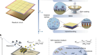
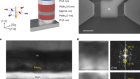
A film of lead sulfide — an infrared-sensitive semiconductor — has been grown directly on a circuit that can read out the material’s electrical signal through an approach called monolithic in situ integration. This brings material growth and electronic integration together into a single step. The resulting image sensor shows high sensitivity for infrared wavelengths.
This is a summary of: Li, S. et al . Monolithically and in situ integrated PbS infrared imagers. Nature 659 , 83–90 (2026) .
doi: https://doi.org/10.1038/d41586-026-03420-5
‘Expert opinion’ is published under a CC BY 4.0 licence.
References
Wuu, S.-G. et al. IEEE Trans. Electron Devices 69 , 2766–2778 (2022).
Article Google Scholar
Liu, J. et al. Nature Electron. 5 , 443–451 (2022).
Article Google Scholar
Arslan, Y., Oguz, F. & Besikci, C. IEEE J. Quantum Electron. 50 , 957–964 (2014).
Article Google Scholar
Kim, K. S. et al.…