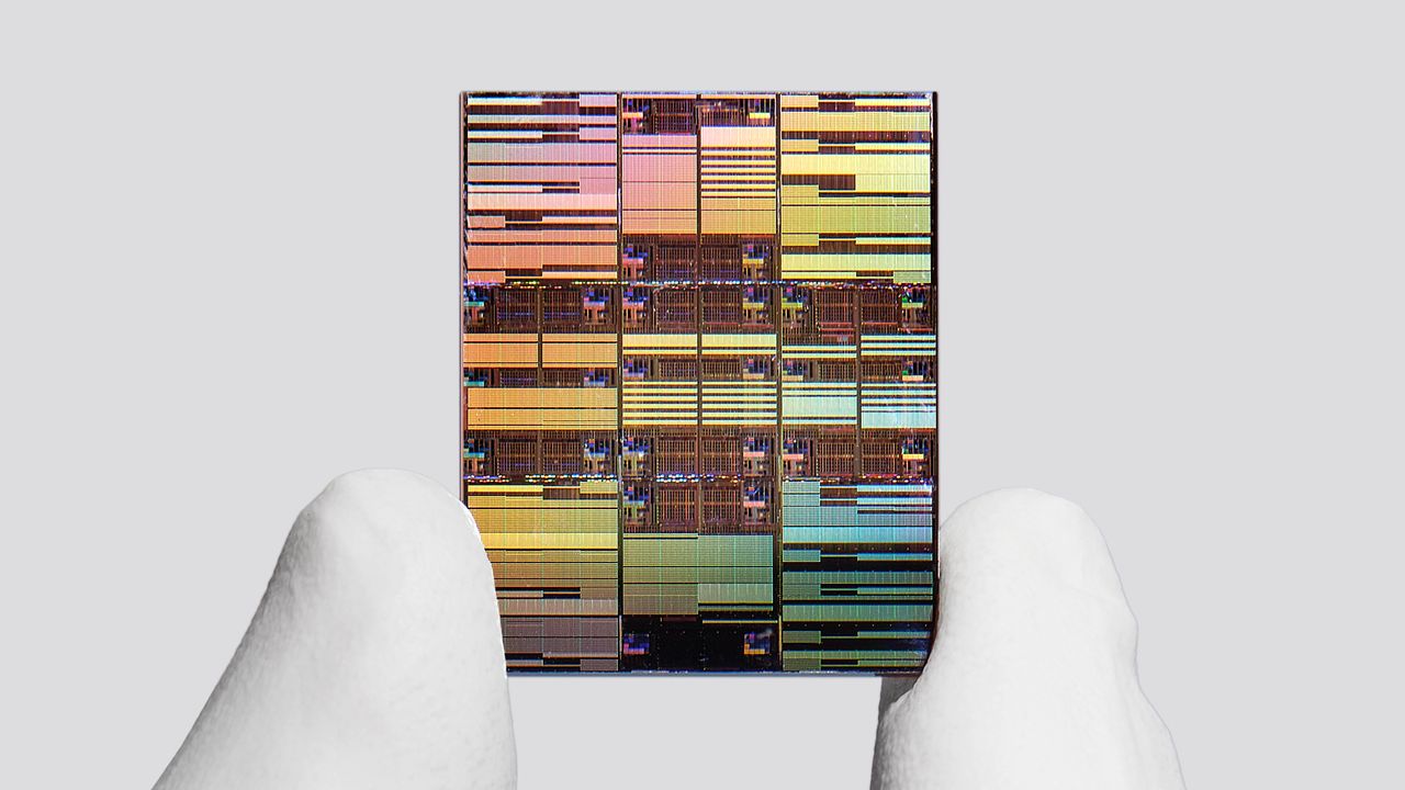
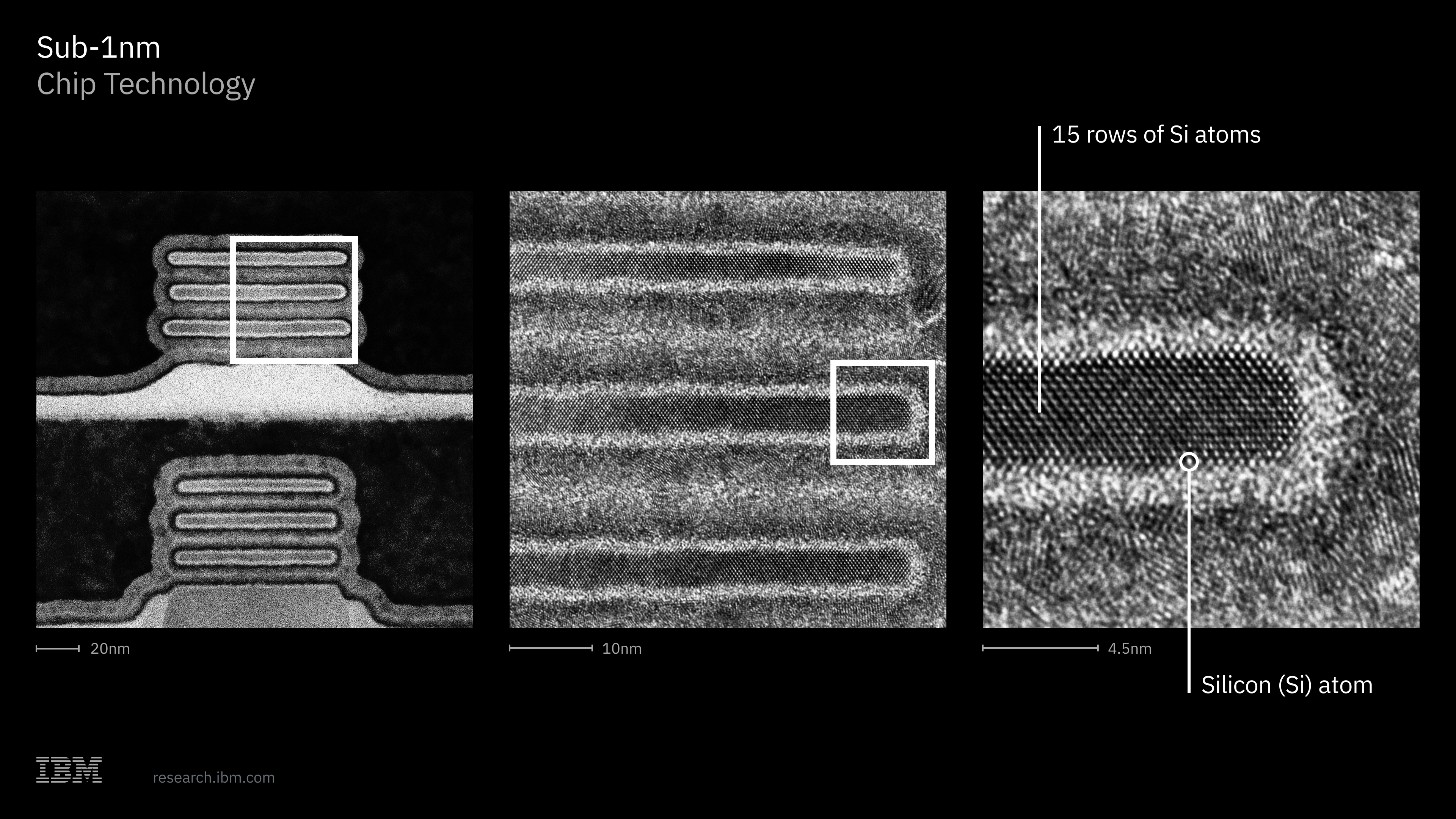
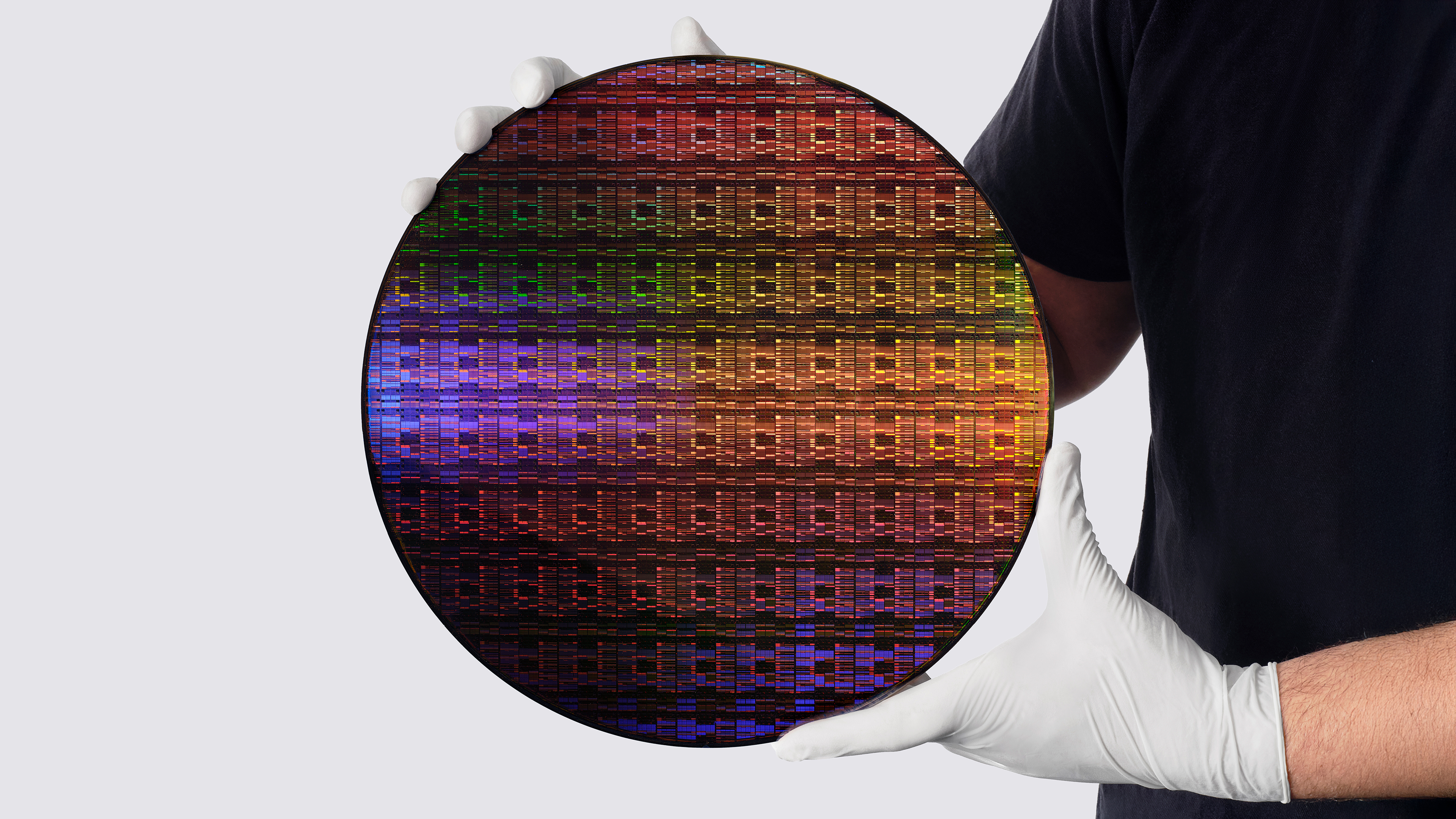
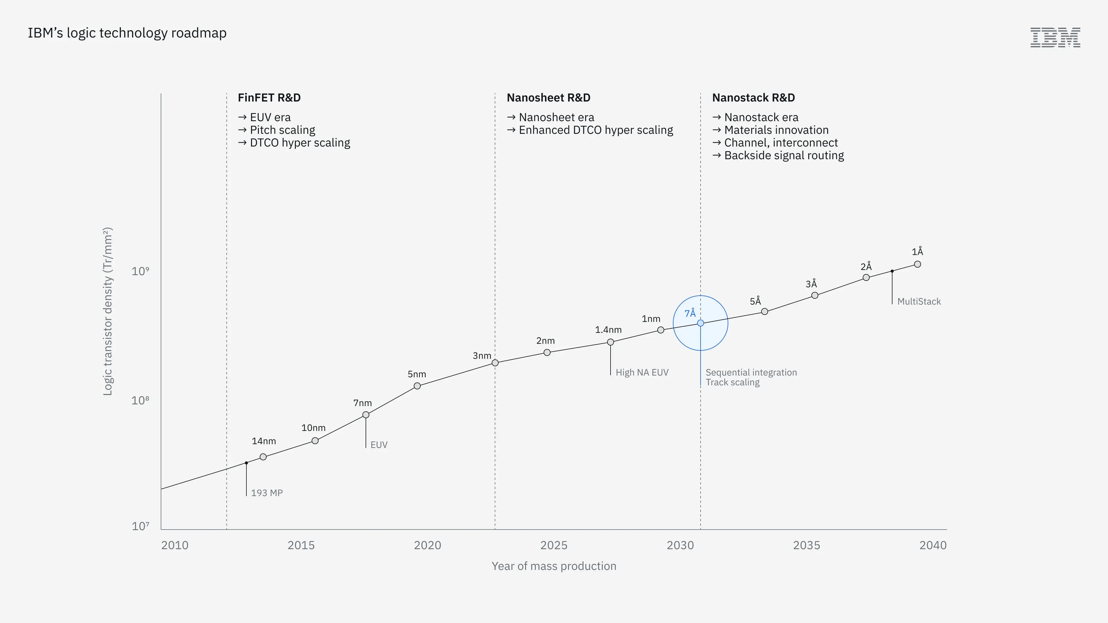
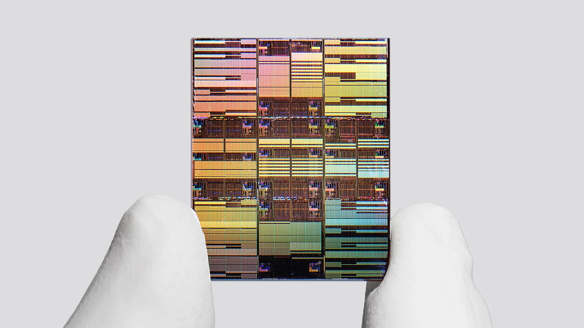
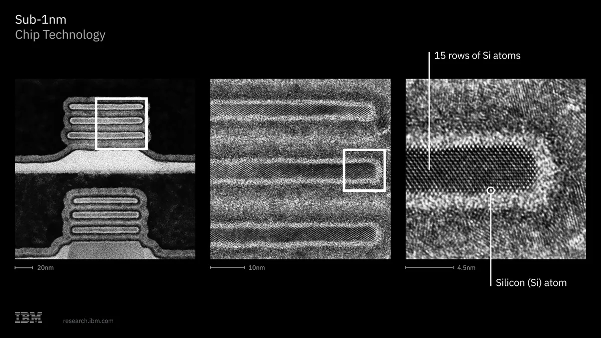
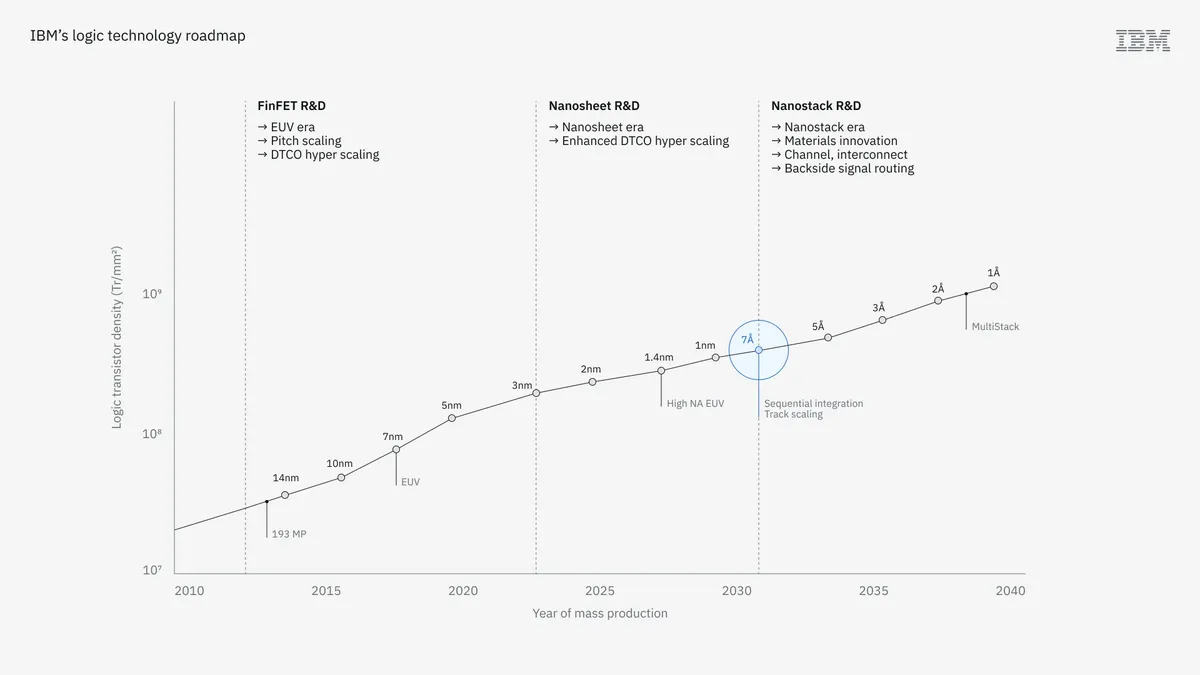
(Image credit: IBM) IBM on Thursday said it has produced the first test chip using its 0.7nm-class (7 angstroms) fabrication technology , the industry's first sub-1nm manufacturing process. The concept process technology relies on the so-called nanostack transistors and promises rather dramatic power, performance, and area (PPA) gains compared to IBM's 2nm-class node. To produce nanostack transistors, IBM uses two wafers instead of one, along with ultra-thin dielectric bonding, an arrangement that has never been used before. IBM's 7A-class (or 0.7nm-class) fabrication process based on nanostack transistors is said to offer up to 50% higher performance and 70% higher energy efficiency compared to IBM's 2nm-class node based on nanosheet gate-all-around transistors the company introduced in 2021. Perhaps more importantly, IBM's nanosheet architecture provides a 40% higher SRAM density and even higher density improvements for logic transistors, gains that are extremely hard to achieve these days.…